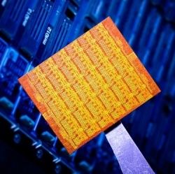
A team of researchers from Taiwan and the University of California, Berkeley, has harnessed nanodots to create a new electronic memory technology that can write and erase data 10-100 times faster than today’s mainstream charge-storage memory products. The new system uses a layer of non-conducting material embedded with discrete (non-overlapping) silicon nanodots, each approximately 3 nanometers across. Each nanodot functions as a single memory bit. To control the memory operation, this layer is then covered with a thin metallic layer, which functions as a “metal gate.” The metal gate controls the “on” and “off” states of the transistor.
Applied Physics Letters – Fast programming metal-gate Si quantum dot nonvolatile memory using green nanosecond laser spike annealing
The ultrafast metal-gate silicon quantum-dot (Si-QD) nonvolatile memory (NVM) with program/erase speed of 1 μs under low operating voltages of ± 7 V is achieved by thin tunneling oxide, in situ Si-QD-embedded dielectrics, and metal gate. Selective source/drain activation by green nanosecond laser spike annealing, due to metal-gate as light-blocking layer, responds to low thermal damage on gate structures and, therefore, suppresses re-crystallization/deformation/diffusion of embedded Si-QDs. Accordingly, it greatly sustains efficient charge trapping/de-trapping in numerous deep charge-trapping sites in discrete Si-QDs. Such a gate nanostructure also ensures excellent endurance and retention in the microsecond-operation Si-QD NVM.
The researchers were able to achieve this new milestone in speed by using ultra-short bursts of green laser light to selectively anneal (activate) specific regions around the metal layer of the metal gate of the memory. Since the sub-millisecond bursts of laser light are so brief and so precise, they are able to accurately create gates over each of the nanodots. This method of memory storage is particularly robust, the researchers explain, because if an individual charge in one of the nano-sites failed, it would barely influence the others. This enables a stable and long-lived data storage platform.
“The materials and the processes used for the devices are also compatible with current main-stream integrated circuit technologies,” explains Shieh. “This technology not only meets the current CMOS process line, but can also be applied to other advanced-structure devices.”