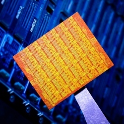
Microelectromechanical systems, or MEMS, are small devices with huge potential. Typically made of components less than 100 microns in size — the diameter of a human hair — they have been used as tiny biological sensors, accelerometers, gyroscopes and actuators.
For the most part, existing MEMS devices are two-dimensional, with functional elements engineered on the surface of a chip. It was thought that operating in three dimensions — to detect acceleration, for example — would require complex manufacturing and costly merging of multiple devices in precise orientations.
The new silicon device contains microscopic elements about the width of a red blood cell that can be engineered to reach heights of hundreds of microns above the chip’s surface.
Fabio Fachin, a postdoc in the Department of Aeronautics and Astronautics, says the chip can be outfitted with sensors, placed atop and underneath the chip’s minuscule bridges, to detect three-dimensional phenomena such as acceleration. Such a compact accelerometer may be useful in several applications, including autonomous space navigation, where extremely accurate resolution of three-dimensional acceleration fields is key.
“One of the main driving factors in the current MEMS industry is to try to make fully three-dimensional devices on a single chip, which would not only enable real 3-D sensing and actuation, but also yield significant cost benefits,” Fachin says. “A MEMS accelerometer could give you very accurate acceleration [measurements] with a very small footprint, which in space is critical.”
Moving to 3D
While most MEMS devices are two-dimensional, there have been efforts to move the field into 3-D, particularly for devices made from polymers. Scientists have used lithography to fabricate intricate, three-dimensional structures from polymers, which have been used as tiny gears, cogs and micro-turbines. However, Fachin says, polymers lack the stiffness and strength required for some applications, and can deform at high temperatures — qualities that are less than ideal in applications like actuators and shock absorbers.
By contrast, materials such as silicon are relatively durable and temperature-resistant. But, Fachin says, fabricating 3-D devices in silicon is tricky. MEMS engineers use a common technique called deep reactive ion etching to make partially 3-D structures, in which two-dimensional elements are etched into a wafer. The technique, however, does not enable full 3-D configurations, where structures rise above a chip’s surface.
To make such devices, engineers fabricate tiny two-dimensional bridges, or cantilevers, on a chip’s surface. After the chip is produced, they apply a small force to arch the bridge into a three-dimensional configuration. This last step, Fachin says, requires great precision.