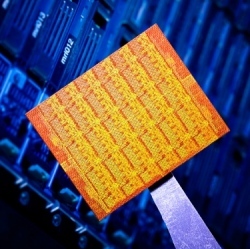
The chip giant is currently ramping its 22nm process with third-generation Core chips known as Ivy Bridge that were first released in late 2011. Comfortably ensconced in the high-volume stage of 22nm production, Bohr said defect density in Intel’s 22nm silicon have improved considerably and yields are now matching the previous 32nm generation of products.
Bohr said extreme ultraviolet (EUV) lithography would be preferable for the 10nm node, but it probably wouldn’t be cost-effective at that point.
Beyond 10nm, Intel has pegged 7nm and 5nm transistors as the next stops on the Moore’s Law-driven path to ever-smaller circuitry packed more densely onto computer chips every 18 months or so.
Intel’s most far-reaching researchers are now experimenting with to achieve process technologies beyond 10nm, but did mention that the carbon allotrope graphene was a material being considered for future transistors.
If the whats and hows of getting to 7nm and beyond aren’t fully resolved, Bohr still expressed full confidence that Intel wouldn’t experience any major hiccups in extended Moore’s Law for another decade.
"Intel’s technology pipeline is full with research extending out 10 years and down to the 10nm, 7nm, and 5nm nodes. It looks like we have a a solution for 10nm and I’m confident we will have solutions for 7nm and 5nm," he said.
Intel is now classifying its process technology advances for two different sorts of end products in its portfolio. On the one hand, there are the performance-maximized chips like Ivy Bridge that are aimed at powerful clients and servers, and on the other there are the low-power System-on-a-Chip designs built for mobile devices and embedded systems.