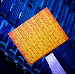
IBM researchers have built a prototype optical chip that can transfer a terabit of data per second, using an innovative design requiring 48 tiny holes drilled into a standard CMOS chip, facilitating the movement of light. Much faster and more power-efficient than today’s optics, the so-called "Holey Optochip" technology could enhance the power of supercomputers.
Optical chips, which move data with light instead of electrons, are commonly used for interconnects in today’s supercomputers and can be found in IBM systems such as Power 775 and Blue Gene. Optical technology is favored over electrical for transmitting high-bandwidth data over longer distances, which is why it’s used for telecommunications networks, said IBM Optical Links Group manager Clint Schow.
As speed and efficiency improve, optical technology has become more viable in smaller settings. "I think the number one supercomputer ten years ago had no optics in it whatsoever, and now you’re seeing large scale deployments, mostly for rack-to-rack interconnects within supercomputers," Schow told Ars. "It’s making its way deeper into the system and getting closer and closer to the actual processor."
With the Holey Optochip, Schow said "our target is the bandwidth that interconnects different processors in the system—not the processor talking to its memory, but a processor talking to another processor in a large parallel system."
The Holey Optochip uses 4.7 watts in delivering nearly one trillion bits per second, enough to download 500 HD movies. At 5.2 mm by 5.8 mm, it’s about one-eighth the size of a dime.
IBM built the chip using standard parts so it can make its way to market relatively quickly. "The heart of the chip is a single CMOS, plain-Jane unmodified process chip," Schow said. "That base chip has all the electronic circuit functions to complete the optical link. So it’s got drivers that modulate vertical cavity lasers and receiver circuits that convert photocurrent from a detector into a usable electrical signal."
Drilling holes into the chip lets IBM use industry-standard, 850-nanometer vertical cavity surface emitting lasers (VCSEL), and photodiode arrays, both soldered on to the chip. The holes allow optical access through the back of the chip to the transmitter and receiver channels, making it more compact.
"You need the holes because if you have the silicon substrate the chip is made out of, the light can’t go through it," Schow said. "You need to make a hole to let the light pass through." An IBM spokesperson further explains that "the optical devices are directly soldered to the front of the CMOS IC (integrated circuit) and the emission/detection of the optical signals is pointed toward the back of the chip. The holes are etched through the chip, one under each laser and detector to allow the optical signals to pass through the chip itself."